线缆
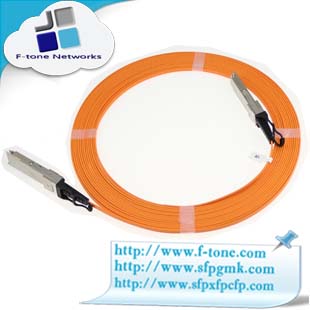
120Gbps CXP有源光缆AOC
Description
F- tone公司专业研发制造120Gbps CXP有源光缆AOC、120G CXP Active Optical Cable, 符合SFF-8648/EIA-965应用于100G以太网和InfiniBand FDR等数据中心互联场景。100%完美兼容全系列品牌服务器,交换机,路由器,PDH/SDH传输设 备,EPON,GPON,10G EPON,10G GPON,WDM PON基站等等全系列设备
QSFP+ Active Optical Cable
Features
¨ Full duplex 4 channel 850nm parallel active optical cable
¨ Transmission data rate up to 10.3Gbit/s per channel
¨ SFF-8436 QSFP+ compliant
¨ Hot pluggable electrical interface
¨ Differential AC-coupled high speed data interface
¨ 4 channels 850nm VCSEL array
¨ 4 channels PIN photo detector array
¨ Maximum link length of 300m on OM3 Multimode Fiber (MMF)and 400m on OM4 MMF
¨ Low power consumption <1.5W
¨ Operating case temperature 0°C to +70°C
¨ 3.3V power supply voltage
¨ RoHS 6 compliant
Applications
¨ Infiniband transmission at 4ch SDR, DDR and QDR
¨ 40GBASE-SR4 40G Ethernet
¨ Data Centers
Description
QSFP active optic cables are a high performance, low power consumption, long reach interconnect solution supporting 40G Ethernet, fiber channel and PCIe. It is compliant with the QSFP MSA and IEEE P802.3ba 40GBASE-SR4. F-tone QSFP AOC is an assembly of 4 full-duplex lanes, where each lane is capable of transmitting data at rates up to 10Gb/s, providing an aggregated rate of 40Gb/s.
AOC is one kind of parallel transceiver. VCSEL and PIN array package is key technique, through I2C system can contact with module.
Absolute Maximum Ratings
|
Parameter |
Symbol |
Min |
Max |
Unit |
|
Supply Voltage |
Vcc |
-0.3 |
3.6 |
V |
|
Input Voltage |
Vin |
-0.3 |
Vcc+0.3 |
V |
|
Storage Temperature |
Tst |
-20 |
85 |
ºC |
|
Case Operating Temperature |
Top |
0 |
70 |
ºC |
|
Humidity(non-condensing) |
Rh |
5 |
95 |
% |
Recommended Operating Conditions
|
Parameter |
Symbol |
Min |
Typical |
Max |
Unit |
|
Supply Voltage |
Vcc |
3.13 |
3.3 |
3.47 |
V |
|
Operating Case temperature |
Tca |
0 |
70 |
ºC |
|
|
Data Rate Per Lane |
fd |
2.5 |
10.3 |
Gbps |
|
|
Humidity |
Rh |
5 |
85 |
% |
|
|
Power Dissipation |
Pm |
1.5 |
W |
||
|
Fiber Bend Radius |
Rb |
3 |
cm |
Specifications
|
Parameter |
Symbol |
Min |
Typical |
Max |
Unit |
|
Differential input impedance |
Zin |
90 |
100 |
110 |
ohm |
|
Differential Output impedance |
Zout |
90 |
100 |
110 |
ohm |
|
Differential input voltage amplitude aAmplitude |
ΔVin |
300 |
1100 |
mVp-p |
|
|
Differential output voltage amplitude |
ΔVout |
500 |
800 |
mVp-p |
|
|
Skew |
Sw |
300 |
ps |
||
|
Bit Error Rate |
BR |
E-12 |
|||
|
Input Logic Level High |
VIH |
2.0 |
VCC |
V |
|
|
Input Logic Level Low |
VIL |
0 |
0.8 |
V |
|
|
Output Logic Level High |
VOH |
VCC-0.5 |
VCC |
V |
|
|
Output Logic Level Low |
VOL |
0 |
0.4 |
V |
Note:
- BER=10^-12; PRBS 2^31-1@10.3125Gbps.
2. Differential input voltage amplitude is measured between TxnP and TxnN
3. Differential output voltage amplitude is measured between RxNP and RxnN
Optical Characteristics
|
Parameter |
Symbol |
Min |
Typical |
Max |
Unit |
Notes |
|
|
Transmitter |
|||||||
|
Centre Wavelength |
λc |
840 |
850 |
860 |
nm |
- |
|
|
RMS spectral width |
∆λ |
- |
- |
0.65 |
nm |
- |
|
|
Average launch power, each lane |
Pout |
-7.5 |
- |
2.5 |
dBm |
- |
|
|
Difference in launch power between any two lanes (OMA) |
4 |
dB |
- |
||||
|
Extinction Ratio |
ER |
3 |
- |
- |
dB |
- |
|
|
Peak power, each lane |
4 |
dBm |
- |
||||
|
ransmitter and dispersion penalty (TDP), each lane |
TDP |
3.5 |
dB |
- |
|||
|
Average launch power of OFF transmitter, each lane |
-30 |
dB |
- |
||||
|
Eye Mask coordinates: X1, X2, X3, Y1, Y2, Y3 |
SPECIFICATION VALUES 0.23, 0.34, 0.43, 0.27, 0.35, 0.4 |
Hit Ratio = 5x10⁻⁵ |
|||||
|
Receiver |
|||||||
|
Centre Wavelength |
λc |
840 |
850 |
860 |
nm |
- |
|
|
Stressed receiver sensitivity in OMA, each lane |
-5.4 |
dBm |
1 |
||||
|
Maximum Average power at receiver input, each lane |
2.4 |
dBm |
- |
||||
|
Receiver Reflectance |
-12 |
dB |
- |
||||
|
Peak power, each lane |
4 |
dBm |
- |
||||
|
LOS Assert |
-30 |
dBm |
- |
||||
|
LOS De-Assert – OMA |
-7.5 |
dBm |
- |
||||
|
LOS Hysteresis |
0.5 |
dB |
- |
||||
Note:
1.Measured with conformance test signal at TP3 for BER = 10e-12
Pin Descriptions
|
Pin |
Logic |
Symbol |
Name/Description |
Ref. |
|
1 |
GND |
Module Ground |
1 |
|
|
2 |
CML-I |
Tx2- |
Transmitter inverted data input |
|
|
3 |
CML-I |
Tx2+ |
Transmitter non-inverted data input |
|
|
4 |
GND |
Module Ground |
1 |
|
|
5 |
CML-I |
Tx4- |
Transmitter inverted data input |
|
|
6 |
CML-I |
Tx4+ |
Transmitter non-inverted data input |
|
|
7 |
GND |
Module Ground |
1 |
|
|
8 |
LVTTL-I |
MODSEIL |
Module Select |
2 |
|
9 |
LVTTL-I |
ResetL |
Module Reset |
2 |
|
10 |
VCCRx |
+3.3v Receiver Power Supply |
||
|
11 |
LVCMOS-I |
SCL |
2-wire Serial interface clock |
2 |
|
12 |
LVCMOS-I/O |
SDA |
2-wire Serial interface data |
2 |
|
13 |
GND |
Module Ground |
1 |
|
|
14 |
CML-O |
RX3+ |
Receiver non-inverted data output |
|
|
15 |
CML-O |
RX3- |
Receiver inverted data output |
|
|
16 |
GND |
Module Ground |
1 |
|
|
17 |
CML-O |
RX1+ |
Receiver non-inverted data output |
|
|
18 |
CML-O |
RX1- |
Receiver inverted data output |
|
|
19 |
GND |
Module Ground |
1 |
|
|
20 |
GND |
Module Ground |
1 |
|
|
21 |
CML-O |
RX2- |
Receiver inverted data output |
|
|
22 |
CML-O |
RX2+ |
Receiver non-inverted data output |
|
|
23 |
GND |
Module Ground |
1 |
|
|
24 |
CML-O |
RX4- |
Receiver inverted data output |
|
|
25 |
CML-O |
RX4+ |
Receiver non-inverted data output |
|
|
26 |
GND |
Module Ground |
1 |
|
|
27 |
LVTTL-O |
ModPrsL |
Module Present, internal pulled down to GND |
|
|
28 |
LVTTL-O |
IntL |
Interrupt output, should be pulled up on host board |
2 |
|
29 |
VCCTx |
+3.3v Transmitter Power Supply |
||
|
30 |
VCC1 |
+3.3v Power Supply |
||
|
31 |
LVTTL-I |
LPMode |
Low Power Mode |
2 |
|
32 |
GND |
Module Ground |
1 |
|
|
33 |
CML-I |
Tx3+ |
Transmitter non-inverted data input |
|
|
34 |
CML-I |
Tx3- |
Transmitter inverted data input |
|
|
35 |
GND |
Module Ground |
1 |
|
|
36 |
CML-I |
Tx1+ |
Transmitter non-inverted data input |
|
|
37 |
CML-I |
Tx1- |
Transmitter inverted data input |
|
|
38 |
GND |
Module Ground |
1 |
Notes:
1. Module circuit ground is isolated from module chassis ground within the module.
2. Open collector; should be pulled up with 4.7k – 10k ohms on host board to a voltage between 3.15Vand 3.6V.
ModSelL Pin
The ModSelL is an input pin. When held low by the host, the module responds to 2-wire serial communication
commands. The ModSelL allows the use of multiple QSFP modules on a single 2-wire interface bus. When
the ModSelL is “High”, the module will not respond to any 2-wire interface communication from the host.
ModSelL has an internal pull-up in the module.
ResetL Pin
Reset. LPMode_Reset has an internal pull-up in the module. A low level on the ResetL pin for longer than the
minimum pulse length (t_Reset_init) initiates a complete module reset, returning all user module settings to
their default state. Module Reset Assert Time (t_init) starts on the rising edge after the low level on the
ResetL pin is released. During the execution of a reset (t_init) the host shall disregard all status bits until the
module indicates a completion of the reset interrupt. The module indicates this by posting an IntL signal with
the Data_Not_Ready bit negated. Note that on power up (including hot insertion) the module will post this
completion of reset interrupt without requiring a reset.
LPMode Pin
F-tone QSFP AOC operate in the low power mode (less than 1.5 W power consumption)
This pin active high will decrease power consumption to less than 1W.
ModPrsL Pin
ModPrsL is pulled up to Vcc on the host board and grounded in the module. The ModPrsL is asserted “Low”
when the module is inserted and deasserted “High” when the module is physically absent from the host connector.
IntL Pin
IntL is an output pin. When “Low”, it indicates a possible module operational fault or a status critical to the
host system. The host identifies the source of the interrupt by using the 2-wire serial interface. The IntL pin is
an open collector output and must be pulled up to Vcc on the host board.
DIAGNOSTIC MONITORING INTERFACE
Digital diagnostics monitoring function is available on all F-tone QSFP AOCs. A 2-wire serial interface
provides user to contact with module.
The structure of the memory is shown in Figure 4. The memory space is arranged into a lower, single page, address space of 128 bytes and multiple upper address space pages. This structure permits timely access to addresses in the lower page, such as Interrupt Flags and Monitors. Less time critical time entries, such as serial ID information and threshold settings, are available with the Page Select function.
The interface address used is A0xh and is mainly used for time critical data like interrupt handling in order to enable a one-time-read for all data related to an interrupt situation. After an interrupt, IntL, has been asserted, the host can read out the flag field to determine the affected channel and type of flag.
Page02 is User EEPROM and its format decided by user.
The detail description of low memory and page00.page03 upper memory please see SFF-8436 document.
Timing for Soft Control and Status Functions
|
Parameter |
Symbol |
Max |
Unit |
Conditions |
|
Initialization Time |
t_init |
2000 |
ms |
Time from power on1, hot plug or rising edge of Reset until the module is fully functional2 |
|
Reset Init Assert Time |
t_reset_init |
2 |
μs |
A Reset is generated by a low level longer than the minimum reset pulse time present on the ResetL pin. |
|
Serial Bus Hardware Ready Time |
t_serial |
2000 |
ms |
Time from power on1 until module responds to data transmission over the 2-wire serial bus |
|
Monitor Data Ready Time |
t_data |
2000 |
ms |
Time from power on1 to data not ready, bit 0 of Byte 2, deasserted and IntL asserted |
|
Reset Assert Time |
t_reset |
2000 |
ms |
Time from rising edge on the ResetL pin until the module is fully functional2 |
|
LPMode Assert Time |
ton_LPMode |
100 |
μs |
Time from assertion of LPMode (Vin:LPMode = Vih) until module power consumption enters lower Power Level |
|
IntL Assert Time |
ton_IntL |
200 |
ms |
Time from occurrence of condition triggering IntL until Vout:IntL = Vol |
|
IntL Deassert Time |
toff_IntL |
500 |
μs |
Time from clear on read3 operation of associated flag until Vout:IntL = Voh. This includes deassert times for Rx LOS, Tx Fault and other flag bits. |
|
Rx LOS Assert Time |
ton_los |
100 |
ms |
Time from Rx LOS state to Rx LOS bit set and IntL asserted |
|
Tx Fault Assert Time |
ton_Txfault |
200 |
ms |
Time from Tx Fault state to Tx Fault bit set and IntL asserted |
|
Flag Assert Time |
ton_flag |
200 |
ms |
Time from occurrence of condition triggering flag to associated flag bit set and IntL asserted |
|
Mask Assert Time |
ton_mask |
100 |
ms |
Time from mask bit set4 until associated IntL assertion is inhibited |
|
Mask Deassert Time |
toff_mask |
100 |
ms |
Time from mask bit cleared4 until associated IntlL operation resumes |
|
ModSelL Assert Time |
ton_ModSelL |
100 |
μs |
Time from assertion of ModSelL until module responds to data transmission over the 2-wire serial bus |
|
ModSelL Deassert Time |
toff_ModSelL |
100 |
μs |
Time from deassertion of ModSelL until the module does not respond to data transmission over the 2-wire serial bus |
|
Power_over-ride or Power-set Assert Time |
ton_Pdown |
100 |
ms |
Time from P_Down bit set 4 until module power consumption enters lower Power Level |
|
Power_over-ride or Power-set Deassert Time |
toff_Pdown |
300 |
ms |
Time from P_Down bit cleared4 until the module is fully functional3 |
Note:
1. Power on is defined as the instant when supply voltages reach and remain at or above the minimum specified value.
2. Fully functional is defined as IntL asserted due to data not ready bit, bit 0 byte 2 deasserted.
3. Measured from falling clock edge after stop bit of read transaction.
4. Measured from falling clock edge after stop bit of write transaction.
Figure8.Timing Specifications
Mechanical Dimensions
Figure9.Mechanical Specifications
Ordering information
|
Part Number |
Product Description |
|
QSFP-40GAOC-XXX |
XXX=different cable lengths on OM3 Multimode Fiber (MMF) |
|
XX(X) |
Cable Length on OM3 Multimode Fiber (MMF) |
|
03 |
003=3m |
|
05 |
005=5m |
|
10 |
010=10m |
|
20 |
020=20m |
|
50 |
050=50m |
|
300 |
300=300m |
References
1. SFF-8436 QSFP+
2. Infiniband IB-4x-SX, IB-4x-DDR-SX, IB-4x-QDR-SX
3. Ethernet 40GBASE-SR4