标准光模块

10Gbps MiniSFF CWDM Transceiver
Description
FEATURES
● Surface mount I/O pins for high speed signal integrity
● All metal body, solder or screw mount options
● Industrial Temp range, vibration tolerant design
● Up to 10km links
● 2-Fiber MiniSFF LC Transceiver
● 1271~1611nm CWDM Cooled DML transmitter
● Multimode 850nm Receiver
● Single 3.3V Power Supply
● Operating case temperature:
FT-95-RS-CxxR851X-02D : 0℃~+70℃
FT-95-RS-CxxR851X-02DI : -40℃~+85℃
APPLICATIONS
● CWDM optic fiber transmission system
CWDM optic fiber transmission system
|
AbsoluteMaximumRatings |
|||||
|
Parameter |
Symbol |
Min. |
Max. |
Units |
Note |
|
StorageTemperature |
Ts |
-40 |
85 |
℃ |
- |
|
PowerSupplyVoltage |
Vcc |
-0.5 |
4 |
V |
- |
|
SolderingTemperature |
- |
- |
260 |
℃ |
10 seconds on leads only |
|
InputVoltage |
Vin |
GND |
Vcc |
V |
- |
|
RecommendedOperatingConditions |
|||||
|
Parameter |
Symbol |
Min. |
Typ. |
Max. |
Units |
|
PowerSupplyVoltage |
Vcc |
3.1 |
3.3 |
3.5 |
V |
|
Operating Temperature |
Industrial |
-40 |
- |
85 |
℃ |
|
Standard |
0 |
- |
70 |
℃ |
|
|
DataRate |
- |
- |
10 |
- |
Gbps |
|
PowerSupplyCurrent |
Icc |
- |
- |
450 |
mA |
|
TransmitterSpecifications(3.1V<Vcc<3.5V) |
|||||
|
Parameter |
Symbol |
Min. |
Typ. |
Max. |
Units |
|
Optical |
|||||
|
Center Wavelength |
λC |
λ-6.5 |
|
λ+6.5 |
nm |
|
spectral width |
Δλ |
|
|
1 |
nm |
|
Average Optical Output Power |
Po |
-3 |
- |
+2 |
dBm |
|
Laser Off Power |
Poff |
- |
- |
-30 |
dBm |
|
ExtinctionRatio |
ER |
3.5 |
- |
- |
dB |
|
Side Mode Suppression Ratio |
SMSR |
30 |
- |
- |
dB |
|
Electrical |
|||||
|
DifferentialInputVoltage |
VIH-VIL |
0.3 |
- |
2.2 |
V |
|
ReceiverSpecifications(-3.1V<Vcc<3.5V) |
||||||
|
Parameter |
Symbol |
Min. |
Typ. |
Max. |
Units |
NOTE |
|
Optical |
|
|||||
|
Receiver Sensitivity |
Sen |
- |
- |
-10 |
dBm |
1 |
|
MaximumInputPower(Saturation) |
PMAX |
0 |
- |
- |
dBm |
|
|
SignalDetect--Asserted |
Pa |
- |
- |
-11 |
dBm |
|
|
SignalDetect--Deasserted |
Pd |
-30 |
- |
- |
dBm |
|
|
SignalDetect--Hysteresis |
Phys |
0.5 |
- |
- |
dB |
|
|
WavelengthofOperation |
λ |
700 |
|
900 |
nm |
|
|
Electrical |
|
|||||
|
DifferentialOutputVoltage |
VOH–VOL |
0.4 |
- |
2 |
V |
|
Note1:Measured with average power; BER < 10-12 and PRBS 231 -1.
Digital Diagnostic Memory Map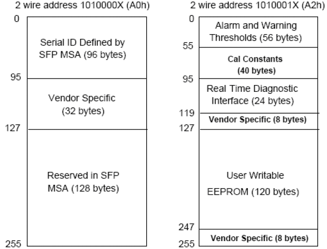
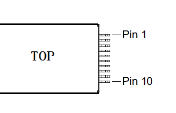
Pins Assignment
Function definition
|
PIN No. |
Name |
Function |
Voltage Level |
|
1 |
TD+ |
Data IN+ |
CML |
|
2 |
VEETX |
Transmitter GND |
N/A |
|
3 |
TD- |
Data IN- |
CML |
|
4 |
VCCTX |
Transmitter VCC |
N/A |
|
5 |
SDA |
The data line of two wire serial interface |
OpenDrain |
|
6 |
SCL |
The clock line of two wire serial interface |
Open Drain |
|
7 |
RD+ |
Data OUT+ |
CML |
|
8 |
VCCRX |
Receiver VCC |
N/A |
|
9 |
RD- |
Data OUT- |
CML |
|
10 |
VEERX |
Receiver GND |
N/A |
Recommended Circuit
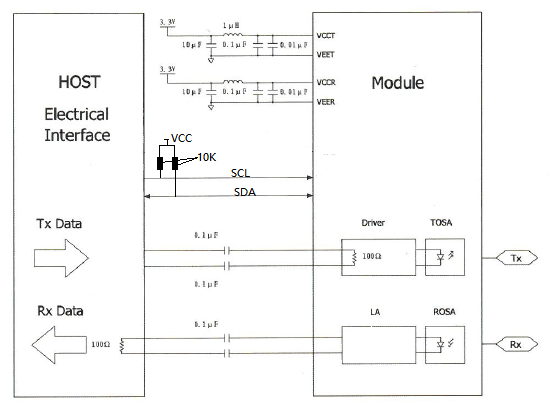
Notes:
1) L1 and L2 = MuRata BLM21A601S or equivalent (600Ω at 100MGz or better).
2) Route the differential pairs (TX +/- and RX +/-) together using 100Ω impedance matched traces.
3) Use separate power supply filtering for VCCT and VCCR, as shown.
Outline Specification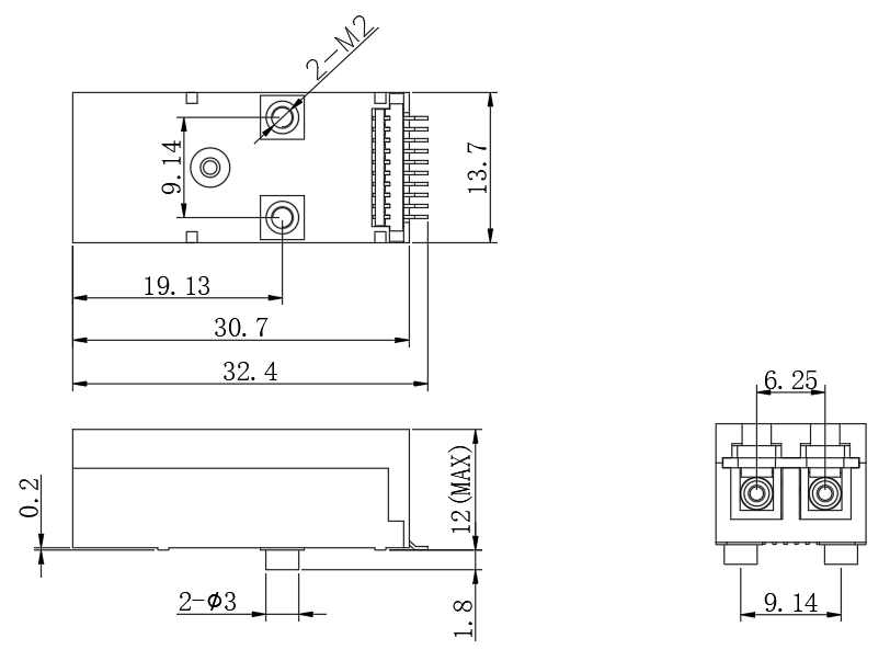
NOTE: Unspecified tolerance:± 0.25mm
Recommended PCB Layout
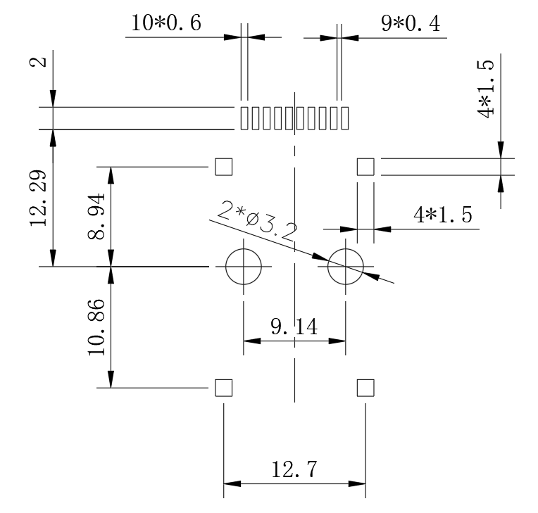
NOTE: Unspecified tolerance:± 0.25mm
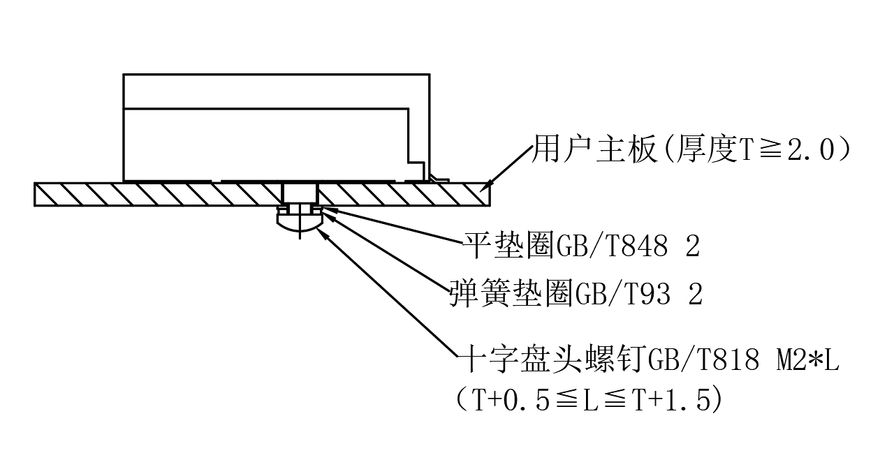
Installation Diagram
Ordering Information
FT-95-RS-CxxR851X-02D XX: 1271~1611nm CWDM Wavelength
|
P/No. |
Temp. (℃) |
Wavelength (nm) |
Dist. (km) |
TX Power (dBm) |
RX Sens (dBm) @850nm |
Package |
Bit Rate (Gb/s) |
Volt. (V) |
|
FT-95-RS-C27R851X-02D |
0~70 |
1271 |
10 |
-3 to +2 |
-10 |
LC |
10 |
3.3 |
|
FT-95-RS-C29R851X-02D |
0~70 |
1291 |
||||||
|
FT-95-RS-C31R851X-02D |
0~70 |
1311 |
||||||
|
FT-95-RS-C33R851X-02D |
0~70 |
1331 |
||||||
|
FT-95-RS-C35R851X-02D |
0~70 |
1351 |
||||||
|
FT-95-RS-C37R851X-02D |
0~70 |
1371 |
||||||
|
FT-95-RS-C39R851X-02D |
0~70 |
1391 |
||||||
|
FT-95-RS-C41R851X-02D |
0~70 |
1411 |
||||||
|
FT-95-RS-C43R851X-02D |
0~70 |
1431 |
||||||
|
FT-95-RS-C45R851X-02D |
0~70 |
1451 |
||||||
|
FT-95-RS-C47R851X-02D |
0~70 |
1471 |
||||||
|
FT-95-RS-C49R851X-02D |
0~70 |
1491 |
||||||
|
FT-95-RS-C51R851X-02D |
0~70 |
1511 |
||||||
|
FT-95-RS-C53R851X-02D |
0~70 |
1531 |
||||||
|
FT-95-RS-C55R851X-02D |
0~70 |
1551 |
||||||
|
FT-95-RS-C57R851X-02D |
0~70 |
1571 |
||||||
|
FT-95-RS-C59R851X-02D |
0~70 |
1591 |
||||||
|
FT-95-RS-C61R851X-02D |
0~70 |
1611 |
FT-95-RS-CxxR851X-02DI XX: 1271~1611nm CWDM Wavelength
|
P/No. |
Temp. (℃) |
Wavelength (nm) |
Dist. (km) |
TX Power (dBm) |
RX Sens (dBm) @850nm |
Package |
Bit Rate (Gb/s) |
Volt. (V) |
|
FT-95-RS-C27R851X-02DI |
-40~85 |
1271 |
10 |
-3 to +2 |
-10 |
LC |
10 |
3.3 |
|
FT-95-RS-C29R851X-02DI |
-40~85 |
1291 |
||||||
|
FT-95-RS-C31R851X-02DI |
-40~85 |
1311 |
||||||
|
FT-95-RS-C33R851X-02DI |
-40~85 |
1331 |
||||||
|
FT-95-RS-C35R851X-02DI |
-40~85 |
1351 |
||||||
|
FT-95-RS-C37R851X-02DI |
-40~85 |
1371 |
||||||
|
FT-95-RS-C39R851X-02DI |
-40~85 |
1391 |
||||||
|
FT-95-RS-C41R851X-02DI |
-40~85 |
1411 |
||||||
|
FT-95-RS-C43R851X-02DI |
-40~85 |
1431 |
||||||
|
FT-95-RS-C45R851X-02DI |
-40~85 |
1451 |
||||||
|
FT-95-RS-C47R851X-02DI |
-40~85 |
1471 |
||||||
|
FT-95-RS-C49R851X-02DI |
-40~85 |
1491 |
||||||
|
FT-95-RS-C51R851X-02DI |
-40~85 |
1511 |
||||||
|
FT-95-RS-C53R851X-02DI |
-40~85 |
1531 |
||||||
|
FT-95-RS-C55R851X-02DI |
-40~85 |
1551 |
||||||
|
FT-95-RS-C57R851X-02DI |
-40~85 |
1571 |
||||||
|
FT-95-RS-C59R851X-02DI |
-40~85 |
1591 |
||||||
|
FT-95-RS-C61R851X-02DI |
-40~85 |
1611 |
Important Notice
Performance figures, data and any illustrative material provided in this data sheet are typical and must be specifically confirmed in writing by F-tone Networks before they become applicable to any particular order or contract. In accordance with the F-tone Networks policy of continuous improvement specifications may change without notice.
The publication of information in this data sheet does not imply freedom from patent or other protective rights of F-tone Networks or others. Further details are available from any F-tone Networks sales representative.
Related Products

400G QSFP56 DD to 8x53G SFP56 Breakout Active Optical Cable
400G QSFP56 DD to 8x53G SFP56 Breakout Active Optical Cable


IP68防水连接器
IP68防水连接器
此款防水连接器具有IP68防水等级和UL94-V0阻燃等级认证,可为客户提供SC、LC、MPO光纤接口,是光纤到天线FTTA解决方案的理想产品。该产品与传统光纤跳线的最大区别在于便携防水对接及光缆抗拉,使用特别设计的用于户外恶劣环境下和光设备对接的材料,以达到防潮防晒等功能。

")
10Gbps MiniSFF LC Transceiver (300m)
10Gbps MiniSFF LC Transceiver (300m)
FEATURES
● Surface mount I/O pins for high speed signal integrity
● All metal body, solder or screw mount options
● Industrial Temp range, vibration tolerant design