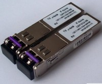
标准光模块

1.25Gbps CSFP 20km
Specifications
- 产品型号: CSFP-OC24-20Axx
- 兼容品牌: 全系列
- 封装类型: CSFP
- 传输速率: Operating Data Rate up to 1.25Gbps
- 传输距离: 3~160KM可选
- 发射波长: 1310nm/1550nm/1490nm 可选
- 接收波长: 1310nm/1550nm/1490nm 可选
- 工作温度: 商业级0℃~+70℃/工业级-40℃~+85℃ 可选
- 数字诊断: 带DDM/不带DDM 可选
- 接收灵敏度: 3~160KM可选
- 接收灵敏度: 3~160KM可选
Description
CSFP-OC24-20Axx 1.25Gbps Compact Bi-Di SFP Transceiver, 20km Reach 1310nm TX / 1490 nm RX
Features
- Support 1.25Gbps data links
- 1310nm FP laser and PIN photodetector for 20km transmission
- 2xBi-directional transceivers in 1 SFP transceiver package
- Compliant with CSFP MSA Option 2 and SFF-8472
- Digital Diagnostic Monitoring:
- Internal Calibration or External Calibration
- Compatible with SONET OC-24 system
- Compatible with RoHS
- +3.3V single power supply
- Operating case temperature:
0 to +70°C(Commercial)
-40°C to +85°C (Industrial)
Applications
- SONET OC-24 system
- Gigabit Ethernet
- Fiber Channel
- Switch to Switch interface
- Point to Point FTTH Application
- Other optical transmission systems
Description
The CSFP transceivers are high performance, cost effective modules supporting 1.25Gbps and 20km transmission distance with SMF.The transceiver consists of three sections: a FP laser transmitter, a PIN photodiode integrated with a trans-impedance preamplifier (TIA) and MCU control unit. All modules satisfy class I laser safety requirements.The transceivers are compatible with Compact SFP Multi-Source Agreement (MSA) and SFF-8472. For further information, please refer to SFP MSA.
Absolute Maximum Ratings
Table 1 - Absolute Maximum Ratings
|
Parameter |
Symbol |
Min |
Max |
Unit |
|
Supply Voltage |
Vcc |
-0.5 |
4.5 |
V |
|
Storage Temperature |
Ts |
-40 |
+85 |
°C |
|
Operating Humidity |
- |
5 |
85 |
% |
Recommended Operating Conditions
Table 2 - Recommended Operating Conditions
|
Parameter |
Symbol |
Min |
Typical |
Max |
Unit |
|
|
Operating Case Temperature |
Commercial |
Tc |
0 |
|
+70 |
°C |
|
Industrial |
-40 |
|
+85 |
°C |
||
|
Power Supply Voltage |
Vcc |
3.13 |
3.3 |
3.47 |
V |
|
|
Power Supply Current |
Icc |
|
|
600 |
mA |
|
|
Data Rate |
|
|
1250 |
|
Mbps |
|
Optical and Electrical Characteristics
CSFP-OC24-20Axx: (FP and PIN, 1310nm, 20km Reach)
Table 3 - Optical and Electrical Characteristics
|
Parameter |
Symbol |
Min |
Typical |
Max |
Unit |
Notes |
||
|
Transmitter |
||||||||
|
Centre Wavelength |
λc |
1260 |
1310 |
1360 |
nm |
|
||
|
Spectral Width (RMS) |
∆λ |
|
|
4 |
nm |
|
||
|
Average Output Power |
Pout |
-9 |
|
-3 |
dBm |
1 |
||
|
Extinction Ratio |
ER |
9 |
|
|
dB |
|
||
|
Optical Rise/Fall Time (20%~80%) |
tr/tf |
|
|
0.26 |
ns |
|
||
|
Data Input Swing Differential |
VIN |
400 |
|
1800 |
mV |
2 |
||
|
Input Differential Impedance |
ZIN |
90 |
100 |
110 |
Ω |
|
||
|
TX Disable |
Disable |
|
2.0 |
|
Vcc |
V |
|
|
|
Enable |
|
0 |
|
0.8 |
V |
|
||
|
TX Fault |
Fault |
|
2.0 |
|
Vcc |
V |
|
|
|
Normal |
|
0 |
|
0.8 |
V |
|
||
|
Receiver |
||||||||
|
Centre Wavelength |
λc |
1470 |
|
1510 |
nm |
|
||
|
Receiver Sensitivity |
|
|
|
-23 |
dBm |
3 |
||
|
Receiver Overload |
|
-3 |
|
|
dBm |
3 |
||
|
LOS De-Assert |
LOSD |
|
|
-23 |
dBm |
|
||
|
LOS Assert |
LOSA |
-35 |
|
|
dBm |
|
||
|
LOS Hysteresis |
|
1 |
|
4 |
dB |
|
||
|
Data Output Swing Differential |
Vout |
400 |
|
1800 |
mV |
4 |
||
|
LOS |
High |
2.0 |
|
Vcc |
V |
|
||
|
Low |
|
|
0.8 |
V |
|
|||
Notes:
1. The optical power is launched into SMF.
2. PECL input, internally AC-coupled and terminated.
3. Measured with a PRBS 27-1 test pattern @1250Mbps, BER ≤1×10-12.
4. Internally AC-coupled.
Timing and Electrical
Table 4 - Timing and Electrical
|
Parameter |
Symbol |
Min |
Typical |
Max |
Unit |
|
Tx Disable Negate Time |
t_on |
|
|
1 |
ms |
|
Tx Disable Assert Time |
t_off |
|
|
10 |
µs |
|
Time To Initialize, including Reset of Tx Fault |
t_init |
|
|
300 |
ms |
|
Tx Fault Assert Time |
t_fault |
|
|
100 |
µs |
|
Tx Disable To Reset |
t_reset |
10 |
|
|
µs |
|
LOS Assert Time |
t_loss_on |
|
|
100 |
µs |
|
LOS De-assert Time |
t_loss_off |
|
|
100 |
µs |
|
Serial ID Clock Rate |
f_serial_clock |
|
|
100 |
KHz |
|
MOD_DEF (1,2)-High |
VH |
2 |
|
Vcc |
V |
|
MOD_DEF (1,2)-Low |
VL |
|
|
0.8 |
V |
Diagnostics
Table 5 – Diagnostics Specification
|
Parameter |
Range |
Unit |
Accuracy |
Calibration |
|
Temperature |
0 to +70 |
°C |
±3°C |
Internal / External |
|
Voltage |
3.0 to 3.6 |
V |
±3% |
Internal / External |
|
Bias Current |
0 to 100 |
mA |
±10% |
Internal / External |
|
TX Power |
-9 to -3 |
dBm |
±3dB |
Internal / External |
|
RX Power |
-23 to -3 |
dBm |
±3dB |
Internal / External |
Pin Descriptions
|
Pin |
Name |
Description |
Plug Seq |
Notes |
|
1 |
VEE |
Transceiver ground, common for 2 channels |
|
|
|
2 |
Tx_ Fault |
Open collector/drain output, high signal indicates fault in one of the TX channels |
|
|
|
3 |
TX_DI S1 |
Transmitter disable control of channel 1, high signal disables optical output |
|
|
|
4 |
SDA |
I2C data (SDA) |
|
|
|
5 |
SCL |
I2C clock (SCL) |
|
|
|
6 |
TD-2 |
Inverted transmitter data input of channel 2 (internally AC coupled) |
|
|
|
7 |
TD+2 |
Non-inverted transmitter data input of channel 2 (internally AC coupled) |
|
|
|
8 |
LOS1 |
Open collector/drain output, high signal indicates los of signal in RX channel 1 |
|
|
|
9 |
RD+2 |
Non-inverted receiver data output of channel 2 (internally AC coupled) |
|
|
|
10 |
RD-2 |
Inverted receiver data output of channel 2 (internally AC coupled) |
|
|
|
11 |
VEE |
Transceiver ground, common for 2 channels |
|
|
|
12 |
RD-1 |
Inverted receiver data output of channel 1 (internally AC coupled) |
|
|
|
13 |
RD+1 |
Non-inverted receiver data output of channel 1 (internally AC coupled) |
|
|
|
14 |
LOS2 |
Open collector/drain output, high signal indicates los of signal in RX channel 2 |
|
|
|
15 |
VccR |
Receiver power, common for 2 channels |
|
|
|
16 |
VccT |
Transmitter power, common for 2 channels |
|
|
|
17 |
TX_ DIS2 |
Transmitter disable control of channel 2, high signal disables optical output |
|
|
|
18 |
TD+1 |
Non-inverted transmitter data input of channel 1 (internally AC coupled) |
|
|
|
19 |
TD-1 |
Inverted transmitter data input of channel 1 (internally AC coupled) |
|
|
|
20 |
VEE |
Transceiver ground, common for 2 channels |
|
|
Notes:
Plug Seq.: Pin engagement sequence during hot plugging.
1) TX Fault report transceiver status as following:
TX Fault is an open collector/drain output, which should be pulled up with a 4.7K–10kΩ resistor on the host board. Pull up voltage between 2.0V and VccT, R+0.3V. When high, output indicates a laser fault of some kind either in Channel 1 or Channel 2. The Host shall read Channel 1/2:A2H/AAH: 110 for details: TX Fault from channel 1 if bit 2 is set in [A2H:110]; TX Fault fromchannel 2 if bit 2 is set in [B2H: 110]. Low indicates normal operation. In the low state, the output will be pulled to < 0.8V.
2) TX_disable1, 2 are an input that is used to shut down the transmitter optical output. It is pulled up within the module with a 4.7–10 kΩ resistor. Its states are:
Low (0 – 0.8V): Transmitter on
(>0.8V, < 2.0V): Undefined
High (2.0 to 3.465V): Transmitter Disabled
Open: Transmitter Disabled
- 1,kΩ resistor on the host board. The pull-up voltage shall be VccT or VccR.
Mod-Def 1 is the clock line of two wire serial interface for serial ID
Mod-Def 2 is the data line of two wire serial interface for serial ID
- 1,2is an open collector output, which should be pulled up with a 4.7k~10kΩ Llsignal; L0 indicates normal operation. In the low state, the output will be pulled to less than
5) RD1,2-/+: These are the differential receiver outputs. They are internally AC-coupled 100 differential lines which should be terminated with 100Ω (differential) at the user SERDES.
6) TD1,2-/+: These are the differential transmitter inputs. They are internally AC-coupled, differential lines with 100Ω differential termination inside the module.
Regulatory Compliance
F-tone Networks SFP transceiver is designed to be Class I Laser safety compliant and is certified per the following standards
|
Feature |
Agency |
Standard |
|
Laser Safety |
FDA |
CDRH 21 CFR 1040 annd Laser Notice No. 50 |
|
Product Safety |
BST |
EN 60825-1:2007 EN 60825-2:2004 EN 60950-1:2006 |
|
Environmental protection |
SGS |
RoHS Directive 2002/95/EC |
|
EMC |
CCIC |
EN 55022:2006+A1:2007 EN 55024:1998+A1:2001+A2:2003 |
Ordering information
|
Part Number |
Product Description |
|
CSFP-OC24-20A |
1.25Gbps, Tx1310nm / Rx 1490nm; Compact SFP bidi, 20KM, DDM 0ºC ~ +70ºC |
|
CSFP-OC24-20AI |
1.25Gbps, Tx1310nm / Rx 1490nm; Compact SFP bidi, 20KM, DDM -40°C to +85°C |
Important Notice
Performance figures, data and any illustrative material provided in this data sheet are typical and must be specifically confirmed in writing by F-tone Networks before they become applicable to any particular order or contract. In accordance with the F-tone Networks policy of continuous improvement specifications may change without notice.
The publication of information in this data sheet does not imply freedom from patent or other protective rights of F-tone Networks or others. Further details are available from any F-tone Networks sales representative.


