标准光模块

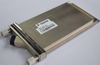
CFP-40G-LR4
Specifications
- 产品型号: CFP-40G-LR4
- 兼容品牌: 全系列
- 封装类型: CFP
- 传输速率: 40G
- 传输距离: Up to 10km over a SMF
- 发射波长: CWDM
- 接收波长: CWDM
- 工作温度: 商业级0℃~+70℃/工业级-40℃~+85℃ 可选
- 数字诊断: 带DDM
- 接收灵敏度: Up to 10km over a SMF
- 接收灵敏度: Up to 10km over a SMF
Description
F-tone 40G CFP LR4 Optical Transceiver Module
Features
- Transmission data rate up to 11.2Gbps per channel
- CFP MSA compliant
- Compliant to IEEE 802.3ba specification for 40GBASE-LR4 links
- OTU3 compatible
- 1310nm Un-cooled CWDM DFB-DML ,Transmitter and optical MUX
- High Sensitivity PIN-TIA and optical DEMUX
- 1271, 1291, 1311, 1331nm CWDM grid in ITU-T G.694.2 up to 10km over a SMF
- MDIO digital diagnostic and control capabilities.
- compliant to CFP MSA Management Interface Specification, Draft 1.4
- TX input and RX output CDR retiming
- Hot pluggable electrical interface
- Power class 1 (<8W max)
- Operating case temperature 0°C to +70°C
- 3.3V power supply
- RoHS 6 compliant(lead free)
Applications
- 40GE Enterprise switches and routers
- Carrier Grade 40GE Core-routers
- CWDM Point to Point and Ring Application
- Other high speed data connections
Description
The CFP optical transceiver module are a high performance, low power consumption, long reach(10 km) interconnect solution supporting 40G Ethernet. It is compliant with the CFP MSA and IEEE P802.3ba 40GBASE-LR4. F-tone CFP 40G LR4 modules offer 4 CWDM transmit and 4 CWDM receive asynchronous channels operating at up to 11.2Gbps per channel.
As shown in Figure 1, the transmitter side of the module consists of an array of VCSELs (Vertical Cavity Surface Emitting Lasers) and associated circuitry, which converts 4 parallel electrical data inputs to 4 parallel optical data output signals and also converts 4 parallel optical signals into 4 parallel electrical signals through an array of PIN photodiodes and associated circuitry.
Absolute Maximum Ratings
|
Parameter |
Symbol |
Min |
Max |
Unit |
|
Supply Voltage |
Vcc |
-0.3 |
3.6 |
V |
|
Input Voltage |
Vin |
-0.3 |
Vcc+0.3 |
V |
|
Storage Temperature |
Tst |
-40 |
85 |
ºC |
|
Case Operating Temperature |
Top |
0 |
70 |
ºC |
|
Humidity(non-condensing) |
Rh |
95 |
% |
Recommended Operating Conditions
|
Parameter |
Symbol |
Min |
Typical |
Max |
Unit |
|
Supply Voltage |
Vcc |
3.13 |
3.3 |
3.47 |
V |
|
Operating Case temperature |
Tca |
0 |
70 |
ºC |
|
|
Data Rate Per Lane |
fd |
- |
11.2 |
Gbps |
|
|
Humidity |
Rh |
85 |
% |
||
|
Power Dissipation |
Pm |
8 |
W |
Electrical Characteristics
|
Parameter |
Symbol |
Min |
Typical |
Max |
Unit |
|
Differential input impedance |
Zin |
90 |
100 |
110 |
ohm |
|
Differential Output impedance |
Zout |
90 |
100 |
110 |
ohm |
|
Differential input voltage amplitude |
ΔVin |
120 |
820 |
mVp-p |
|
|
Differential output voltage amplitude |
ΔVout |
300 |
820 |
mVp-p |
|
|
Input Logic Level High |
VIH |
2.0 |
VCC |
V |
|
|
Input Logic Level Low |
VIL |
0 |
0.8 |
V |
|
|
Output Logic Level High |
VOH |
VCC-0.5 |
VCC |
V |
|
|
Output Logic Level Low |
VOL |
0 |
0.4 |
V |
Note:
1. Differential input voltage amplitude is measured between TxnP and TxnN.
2. Differential output voltage amplitude is measured between RxnP and RxnN.
XLAUI Input Interface
|
XLAUI Receiver Parameters |
symbol |
Min |
Typ |
Max |
Units |
Note |
|
Signal Rate Per Lane |
10.3125 |
Gb/s |
||||
|
Signal Rate tolerance |
-100 |
100 |
ppm |
|||
|
AC Common Mode Voltage Tolerance, RMS |
CMVLTac |
20 |
mV |
|||
|
Minimum Differential Input Return Loss |
Rldiff |
IEEE802.3ba Equation 83B-5 |
dB |
|||
|
Total Input Jitter Tolerance |
Tjin |
0.62 |
UI |
|||
|
Deterministic Input Jitter Tolerance |
Tdin |
0.42 |
UI |
|||
|
Transmitter Input Eye Mask (X1, X2) |
(0.31, 0.5) |
UI |
1 |
|||
|
Transmitter Input Eye Mask (Y1, Y2) |
(42.5, 425) |
mV |
1 |
|||
XLAUI Output Interface
|
XLAUI Driver Parameters |
symbol |
Min |
Typ |
Max |
Units |
Note |
|
Signal Rate Per Lane |
10.3125 |
Gb/s |
||||
|
Signal Rate tolerance |
-100 |
100 |
ppm |
|||
|
Single-end Output Voltage |
Vosingle |
-0.4 |
4 |
V |
||
|
Output AC Common Mode Voltage, RMS |
Vocomac |
15 |
mV |
|||
|
Output Rise and Fall Time (20%-80%) |
Trftl |
24 |
ps |
|||
|
Minimum Differential Output Return Loss |
Rldiff |
IEEE802.3ba Equation 83B-6 |
dB |
|||
|
Total Output Jitter |
Tjo |
0.4 |
UI |
|||
|
Deterministic Output Jitter |
Tdo |
0.25 |
UI |
|||
|
Receiver Output Eye Mask (X1, X2) |
(0.2, 0.5) |
UI |
2 |
|||
|
Receiver Output Eye Mask (Y1, Y2) |
(136, 380) |
mV |
2 |
|||
3.3V CMOS DC parameters
(MOD_RSTn, MOD_LOPWR, TX_DIS, PRG_CNTL, MOD_ABS, RX_LOS, GLB_ALRMn, PRG_ALRM )
|
Parameter |
symbol |
Min |
Typ |
Max |
Units |
Note |
|
Output High Voltage (IOH=-100uA) |
Voh |
Vcc-0.2 |
Vcc+0.3 |
V |
||
|
Output Low Voltage (IOL=100uA) |
Vol |
-0.3 |
0.2 |
V |
||
|
Intput High Voltage |
Vih |
2 |
Vcc+0.3 |
V |
||
|
Input Low Voltage |
Vil |
-0.3 |
0.8 |
V |
||
|
Input Leakage Current |
IIN |
-10 |
10 |
μA |
||
|
Minimun Pulse Width of Control Pin Signal |
t_CNTL |
100 |
μS |
1.2V CMOS DC parameters (MDIO, MDC, PRTADR4:0)
|
Parameter |
symbol |
Min |
Typ |
Max |
Units |
Note |
|
Intput High Voltage |
Vih |
0.84 |
1.5 |
V |
||
|
Input Low Voltage |
Vil |
-0.3 |
0.36 |
V |
||
|
Input Leakage Current |
IIN |
-100 |
100 |
μA |
||
|
Output High Voltage |
Voh |
1.0 |
1.5 |
V |
||
|
Output Low Voltage |
Vol |
-0.3 |
0.2 |
V |
||
|
Output high current (Vi =1.0V) |
Iioh |
-4 |
mA |
|||
|
Output low current (Vi = 0.2V) |
Iol |
4 |
mA |
|||
|
Input Capacitance |
Ci |
10 |
pF |
MDIO and MDC AC parameters
|
Parameter |
symbol |
Min |
Typ |
Max |
Units |
Note |
|
MDC clock Frequency |
fMDC |
0.1 |
4 |
MHz |
||
|
MDC clock period |
tprd |
250 |
10000 |
ns |
||
|
MDIO data hold time |
Thold |
10 |
ns |
|||
|
MDIO data setup time |
Tsetup |
10 |
ns |
|||
|
MDC high and low time |
twidth |
40 |
60 |
% |
||
|
160 |
ns |
|||||
|
Delay from MDC rising edge to MDIO data change |
Tdelay |
175 |
ns |
|||
|
MDIO/MDC termination in CFP |
Zt |
100 |
kOhm |
Optical Characteristics
Transmitter Optical Specifications (T = 25°C, VCC =3.3V +/- 5%)
|
Parameter |
Symbol |
Min |
Typical |
Max |
Unit |
|
Average Optical Power(per channel) |
Pout |
-7 |
2.3 |
dBm |
|
|
Average Optical Power(per channel) - Disabled |
Poff |
-30 |
dBm |
||
|
Optical Return Loss Tolerance |
-12 |
dB |
|||
|
Extinction Ratio |
ER |
3 |
dB |
||
|
Lane0 Wavelength |
λc |
1264.5 |
1271 |
1277.5 |
nm |
|
Lane1 Wavelength |
λc |
1284.5 |
1291 |
1297.5 |
nm |
|
Lane2 Wavelength |
λc |
1304.5 |
1311 |
1317.5 |
nm |
|
Lane3 Wavelength |
λc |
1324.5 |
1331 |
1337.5 |
nm |
|
Side-mode suppression ratio (SMSR) |
SMSR |
30 |
dB |
||
|
Total average launch power |
Ptotal |
8.3 |
dBm |
||
|
Transmitter eye mask definition {X1, X2, X3, Y1, Y2, Y3} |
{0.25, 0.4, 0.45, 0.25, 0.28, 0.4} |
||||
Note:
1. Average optical power is measured at the output of the modules optical interface.
Receiver Optical Specifications (T = 25°C, VCC =3.3V +/- 5%)
|
Parameter |
Symbol |
Min |
Typical |
Max |
Unit |
|
Optical Power Sensitivity(per channel,OMA) |
-11.5 |
dBm |
|||
|
Average receive power, each lane |
Pin max |
2.3 |
dBm |
||
|
Average receive power, each lane |
Pin min |
-13.7 |
dBm |
||
|
Stressed Receiver Sensitivity(OMA) |
PS |
-9.6 |
dBm |
||
|
Receiver reflectance |
λc |
-26 |
dB |
||
|
Difference in receive power between any two lanes (OMA) |
Rl |
7.5 |
dB |
Note:
1. Optical power sensitivity is measured with BER@10<sup< a="">>-12 at 10.3125Gbps per channel.


