Monday - Sunday ( 7x24 hours )
- Call Now
-
028-85255257
- sales@f-tone.com

标准光模块
标准协议光模块
- 全国产化光模块
- 25G~400G高速光模块
- 200km超长距光模块
- 5G移动通信光模块
- SFP光模块
- CWDM SFP
- DWDM SFP
- BIDI-SFP
- SGMII SFP
- Video SFP光模块
- Copper SFP
- 低功耗SFP
- SFP+光模块
- CWDM SFP+
- DWDM SFP+
- BIDI SFP+
- Tunable SFP+
- 16GFC SFP+
- 25GE SFP+
- 32GFC SFP+
- SFP28光模块
- SFP56光模块
- SFP-DD光模块
- QSFP光模块
- QSFP+ 光模块
- QSFP28光模块
- QSFP56光模块
- QSFP112 400G光模块
- QSFP224光模块
- QSFP-DD光模块
- QSFP-DD800光模块
- OSFP 400Gbps
- OSFP 800G光模块
- OSFP 1.6T光模块
- HSFP 1.6T~12.8T光模块
- XFP光模块
- CWDM XFP
- DWDM XFP
- BIDI XFP
- 1x9光模块
- CSFP光模块
- CSFP+10G光模块
- CXP光模块
- CFP光模块
- CFP2光模块
- CFP4光模块
- CFP8 400Gbps
- CDFP 400Gbps
- MicroQSFP光模块
- DSFP光模块
- FT-61光模块
- OLT光模块
- ONU光模块
- PLCC光模块
- RJ光模块
- SFF光模块
- SNAP12光模块
- USOT光模块
- X2光模块
- Xenpak光模块
- 光电编码器模块
- 光模块测试板
- 光模块笼子座子
- DAC 高速线缆
- 光纤滑环|光电滑环
- 光缆车
- 军品级DIN光模块
- 塑料光纤模块
- 替换安华高工业电力光模块
- AD7606国产替代
- 兼容国产化替换安华高光耦
- 射频光模块
- 微型多路光模块
- 特种光模块
- 特种光纤连接器
- 特种光电连接器
- USB光纤延长线
- HDMI
- Mini SAS
- 特种电连接器
- 特种光纤光缆
- 光藕
- SMA测试线缆
- OSA
- PON BOSA
- Pigtailed PD
- RFoG BOSA
- TO-CAN
- 光纤温度传感器
- 光纤应变传感器
- 光纤加速度传感器
- 光线压力传感器
- 光纤位移传感器
- 光纤应力传感器
- 光纤传感分析仪
- 光纤分布式测温主机
- 光纤布里渊信号解调仪
- 分布式光纤声振信号解调仪
- Camera Link
技术支持
兼容协议光模块
- 华为光模块
- 思科光模块
- 华三光模块
- 中航光电光模块
- 中兴光模块
- 锐捷光模块
- 惠普光模块
- 神州数码光模块
- Juniper光模块
- Extreme光模块
- Brocade光模块
- D-Link光模块
- 赫思曼光模块
- 阿尔卡特朗讯光模块
- Allied Telesis光模块
- Foundry光模块
- Force10光模块
- Blade光模块
- Linksys光模块
- Marconi光模块
- 博达光模块
- 网件光模块
- Nortel光模块
- Moxa光模块
- 海康威视HIKVISION光模块
- McAfee光模块
- SMC智邦光模块
- 安华高Avago光模块
- 飞通光模块
- Finisar光模块
- yellobrik SDI光模块
- 罗克韦尔AB光模块
- 罗杰康光模块
- 研华Advantech光模块
其它种类光器件
- 全国产化光器件
- 光纤阵列系列
- 高速模块微连接
- 相干通讯光连接
- 硅光子器件光链接
- Bio-Medical Equipment
- Components for Fiber Laser
- Components for Fiber sensing
- Components for Optical Network
- EDFA光纤放大器
- 光纤传感器
- High power Component
- Hybrid for EDFA
- Test Equipment & Others
- Test Equipment & Others
- 保偏光器件
- 光分路器
- 光开关
- 探测器
- 光功率计
- 全光纤相位拉伸器
- 光纤准直器
- 光衰减器系列
- 光偏振控制器
- 光源
- 光环行器Circulator
- 光纤延迟线
- 色散补偿模块
- 光纤放大器
- 无源传输转换器
- 光纤激光器
- 光调制器
- 薄膜铌酸锂调制器
- 光电探测器
- 光纤偏振
- 光纤滤波器
- 同轴激光器
- 同轴电缆
- 光纤法兰适配器
- 光纤跳线&尾纤
- SMA-特殊纤芯系列
- 特殊接头系列
- 铠装系列
- 光耦合器Coupler
- 皮纤跳线系列
- 大芯数系列
- 回路跳线系列
- 保偏光纤系列
- 光通信组件
- 光隔离器isolator
- 其它光器件
- 可调滤波器
- 可调衰减器
- 拉锥耦合器
- 无源光器件
- 法拉第旋转镜
- 波分复用器
- 滤波器
- 蝶形激光器
- 光耦合器&分路器
- 光纤环形器&法拉第旋转镜
- 光纤隔离器&波分复用器
- 光纤分束器&合束器(PBS/PBC)
- 光纤光栅
- 高速线缆
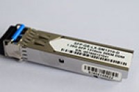
3.125G 单模 1550nm 80km SFP BIDI光模块
Description
3.125G 单模 1550nm 80km SFP BIDI光模块
Features
● 3.125Gb/s serial optical interface
● 1490nm /1550 nm DFB transmitter, photo detector
● 2-wire interface for management specifications compliant with SFF 8472 digital diagnostic monitoring interface for optical transceivers
● Operating case temperature: 0 to 70 °C or-40 to 85 °C
● ll-metal housing for superior EMI performance
● Low power consumption
● Advanced firmware allow customer system encryption information to be stored in transceiver
● Cost effective SFP solution, enables higher port densities and greater bandwidth
● LC connector
● RoHS compliant
Applications
● High-speed networks
● Computer cluster cross-connect
● Custom high-speed data pipes
ABSOLUTEMAXIMUMRATING
These values represent the damage threshold of the module. Stress in excess of any of the individual Absolute Maximum Ratings can cause immediate catastrophic damage to the module even if all other parameters are within Recommended Operating Conditions.
| Parameters | Symbol | Min. | Max. | Unit |
| Power Supply Voltage | VCC | 0 | 3.6 | V |
| Storage Temperature | Tc | -40 | 85 | 。C |
| Operating Case Temperature | Tc | -20 | 85 | 。C |
| TI | -40 | 100 | ||
| Relative Humidity | RH | 5 | 95 | % |
| RX Input Average Power | Pmax | – | -7 | dBm |
Recommended Operating Environment specifies parameters for which the electrical and optical characteristics hold unless otherwise noted.
| Parameters | Symbol | Min. | Typical | Max | Unit |
| Power Supply Voltage | VCC | 3.135 | 3.3 | 3.465 | V |
| Power Supply Current | Icc | 350 | mA | ||
| Operating Temperature | TC | -5 | 25 | 70 | 。C |
| TI | -40 | 25 | 85 |
OPTICAL CHARACTERISTICS
The following optical characteristics are defined over the Recommended Operating Environment unless otherwise specified.
| Parameters | Unit | Values |
| Transmitter | ||
| Center wavelength | nm | 1490/1550 |
| Side Mode Suppression Ratio (min) | dB | 30 |
| Launched power | ||
| – maximum (Average) | dBm | 5 |
| – minimum (Average) | dBm | 0 |
| Transmitter and dispersion penalty (max) | dB | 3.2 |
| Average launch power of OFF transmitter (max) | dBm | -30 |
| Extinction ratio (min) | dB | 6 |
| RIN12 OMA (max) | dB/Hz | -128 |
| Optical Return Loss Tolerance (min) | dB | 12 |
| Receiver | ||
| Center wavelength (range) | nm | 1550/1490 |
| Receive overload (max) in average power(note 1) | dBm | -8 |
| Receive sensitivity (min) in average power(note 1) | dBm | -24 |
| Receiver Reflectance (max) | dB | -12 |
| Vertical eye closure penalty (min)(note 3) | dB | 2.2 |
| Los Threshold (max) | dBm | -40 |
| Los Hysteresis(min) | dB | 0.5 |
| Stressed eye jitter (min)(note 2) | UIp-p | 0.3 |
| Receive electrical 3dB upper cutoff frequency (max) | GHz | 3 |
| Receiver power (damage, Max) | dBm | -7 |
1. Average optical power shall be measured using the methods specified in TIA/EIA-455-95.
2. Power budget is defined as the different between the Rx sensitivity and the Tx output power of the interface.
3. Path penalty is intended as the power penalty of the interface between back-to-back and the maximum applied dispersion.
ELECTRICAL CHARACTERISTICS
The following electrical characteristics are defined over the Recommended Operating Environment unless otherwise specified.
| Parameter | Symbol | Min. | Typical | Max | Unit | Notes |
| Data Rate | – | 3.125 | – | Gbps | ||
| Power Consumption | – | 800 | 1000 | mW | ||
| Transmitter | ||||||
| Single Ended Output Voltage Tolerance | -0.3 | – | 4 | V | ||
| Ccommon mode voltage tolerance | 15 | – | – | mV | ||
| Tx Input Diff Voltage | VI | 100 | 700 | mV | ||
| Tx Fault | VoL | -0.3 | 0.4 | V | At 0.7mA | |
| Data Dependent Input Jitter | DDJ | 0.1 | UI | |||
| Data Input Total Jitter | TJ | 0.28 | UI | |||
| Receiver | ||||||
| Single Ended Output Voltage Tolerance | -0.3 | – | 4 | V | ||
| Rx Output Diff Voltage | Vo | 300 | 850 | mV | ||
| Rx Output Rise and Fall Time | Tr/Tf | 30 | ps | 20% to 80% | ||
| Total Jitter | TJ | 0.7 | UI | |||
| Deterministic Jitter | DJ | 0.42 | UI | |||
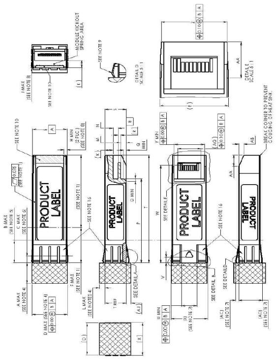
Comply to SFF-8432 rev. 5.0, the improved Pluggable form factor specification.
OrderInformation
| 产品型号 | 封装 | 波长(-xx) | 速率(xx) | 传输距离 (-xx) | x | 等级(x) |
| BYCS-B4531-80Dxx / BYCS-B5431-80Dxx |
SFP+ | B45=T1490/R1550 B54=T1550/R1490 |
31=3.125G | 02≤1.4km 10=10km 20=20km 40=40km 80=80km |
空 不带DDM D 带DDM |
空 商业级 E 扩展级 I 工业级 |
北亿纤通 | F-tone Networks
企业邮箱:sales@f-tone.com
企业网站:www.f-tone.com
企业网站:www.sfpgmk.com
企业电话:028-85255257
企业传真:028-85977702
注:本产品有全国产化型号可选
本产品仅展示部分参数,如有需要,请联系我们。
Important Notice
Performance figures, data and any illustrative material provided in this data sheet are typical and must be specifically confirmed in writing by F-tone Networks before they become applicable to any particular order or contract. In accordance with the F-tone Networks policy of continuous improvement specifications may change without notice.
The publication of information in this data sheet does not imply freedom from patent or other protective rights of F-tone Networks or others. Further details are available from any F-tone Networks sales representative.
Related Products
0~80Mbps MINISFF LVTTL Single Mode Transceiver (10Km)
0~80Mbps MINISFF LVTTL Single Mode Transceiver (10Km)
FEATURES
- All metal body, screw mounting
- 1310 FP transmitter
- MiniSFF FC Pigital Transceiver
SFP 2M DUAL 15KM Transceiver
SFP 2M DUAL 15KM Transceiver
General Description
The SFP transceivers are high performance, cost effective modules supporting data-rate of 2 Mbps and 15km transmission distance on 9/125μm SMF.The transceiver consists of three sections: a laser transmitter, a PIN photodiode integrated with a trans-
光耦合隔离器件
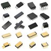
光耦合隔离器件
- 电流转换比 CTR:50~600% (在 IF=5mA, VCE=5V 条件下)
- 输入、输出端之间绝缘电压高 (VISO=3750Vrms)
- 采用 4 引脚微型 SOP 封装结构,
DC-10Mbps 1310nm 20km duplex LC SFP Transceiver
DC-10Mbps 1310nm 20km duplex LC SFP Transceiver
Features
● DC to 10M data rate
● Duplex LC receptacle optical interface compliant
● Single +3.3V power supply
● Hot-pluggable
1250M 单模1310nm 10km SFP BIDI光模块
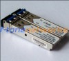
1250M 单模1310nm 10km SFP BIDI光模块
Description
The SFP transceivers are high performance, cost effective modules supporting data rate of 1.25Gbps and 20km transmission distance with SMF.The transceiver consists of three sections: a FP laser transmitter, a PIN photodiode integrated with a trans-impedance
1250M 单模1550nm 20km SFP BIDI光模块
1250M 单模1550nm 20km SFP BIDI光模块
Description
The SFP transceivers are high performance, cost effective modules supporting data rate of 1.25Gbps and 20km transmission distance with SMF.The transceiver consists of three sections: a FP laser transmitter, a PIN photodiode integrated with a trans-impedance